- 您现在的位置:买卖IC网 > Sheet目录223 > ESD11B5.0ST5G (ON Semiconductor)TVS BIDIR 250MW 5V DSN2
ESD11B
Transient Voltage
Suppressors
Micro ? Packaged Diodes for ESD Protection
The ESD11B Series is designed to protect voltage sensitive
XXXX
YYY
components from ESD. Excellent clamping capability, low leakage,
and fast response time provide best in class protection on designs that
are exposed to ESD. Because of its small size, it is suited for use in
cellular phones, MP3 players, digital cameras and many other portable
applications where board space comes at a premium.
Specification Features
? Low Capacitance 12 pF
? Low Clamping Voltage
? Small Body Outline Dimensions: 0.60 mm x 0.30 mm
? Low Body Height: 0.3 mm
? Stand ? off Voltage: 5.0 V
? Low Leakage
? Response Time is < 1 ns
? IEC61000 ? 4 ? 2 Level 4 ESD Protection
? IEC61000 ? 4 ? 4 Level 4 EFT Protection
? These Devices are Pb ? Free, Halogen Free/BFR Free and are RoHS
Compliant
Mechanical Characteristics
MOUNTING POSITION: Any
QUALIFIED MAX REFLOW TEMPERATURE: 260 ° C
Device Meets MSL 1 Requirements
MAXIMUM RATINGS
http://onsemi.com
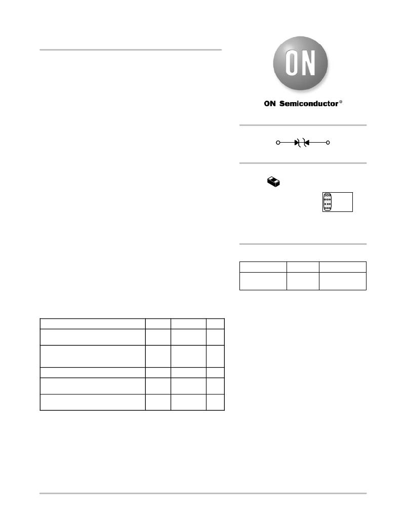
MARKING
DIAGRAM
PIN 1
DSN2
CASE 152AA
XXXX = Specific Device Code
YYY = Year Code
ORDERING INFORMATION
Device Package Shipping ?
ESD11B5.0ST5G DSN2 5000/Tape & Reel
(Pb ? Free)
?For information on tape and reel specifications,
including part orientation and tape sizes, please
refer to our Tape and Reel Packaging Specifications
Brochure, BRD8011/D.
Rating
IEC 61000 ? 4 ? 2 (ESD)
Contact
Air
Symbol
Value
± 15
± 15
Unit
kV
Total Power Dissipation on FR ? 5 Board
(Note 1) @ T A = 25 ° C
Thermal Resistance, Junction ? to ? Ambient
Junction and Storage Temperature Range
Lead Solder Temperature ? Maximum
(10 Second Duration)
Peak Pulse Current, 8 x 20 m s double
exponential waveform (Figure 5)
° P D °
R q JA
T J , T stg
T L
I pp
250
400
? 40 to +125
260
2.0
mW
° C/W
° C
° C
A
Stresses exceeding Maximum Ratings may damage the device. Maximum
Ratings are stress ratings only. Functional operation above the Recommended
Operating Conditions is not implied. Extended exposure to stresses above the
Recommended Operating Conditions may affect device reliability.
1. FR ? 5 = 1.0 x 0.75 x 0.62 in.
See Application Note AND8308/D for further description of survivability specs.
? Semiconductor Components Industries, LLC, 2013
July, 2013 ? Rev. 6
1
Publication Order Number:
ESD11B/D
发布紧急采购,3分钟左右您将得到回复。
相关PDF资料
ESD11L5.0DT5G
TVS ESD UNIDIRECT 150MW SOT-1123
ESD11N5.0ST5G
TVS BIDIR 250MW 5V DSN2
ESD1P0RFWE6327
DIODE RF ESD 1CH SOT323
ESD3V3U1U-02LS E6327
DIODE TVS 3.3V TSSLP-2-1
ESD3V3U4ULC E6327
DIODE TVS 3.3V TSLP-9-1
ESD4238MTTAG
IC ESD CLAMP ARRAY 8CH 16-WDFN
ESD5384NCTBG
DIODE ESD PROTECT 4CH 9-WLCSP
ESD5B5.0ST1G
TVS BIDIRECT 50W SOD523
相关代理商/技术参数
ESD11H120
制造商:Panasonic Industrial Company 功能描述:SWITCH
ESD11L5.0DT5G
功能描述:TVS二极管阵列 LO CAP ESD PROT 5.0V RoHS:否 制造商:Littelfuse 极性: 通道:4 Channels 击穿电压: 钳位电压:11.5 V 工作电压:2.5 V 峰值浪涌电流:20 A 安装风格:SMD/SMT 端接类型:SMD/SMT 系列: 最小工作温度:- 40 C 最大工作温度:+ 85 C
ESD11N5.0ST5G
功能描述:TVS 二极管 - 瞬态电压抑制器 LOW CAP BI DIRECT TV RoHS:否 制造商:Vishay Semiconductors 极性:Bidirectional 工作电压: 击穿电压:58.9 V 钳位电压:77.4 V 峰值浪涌电流:38.8 A 系列: 封装 / 箱体:DO-214AB 最小工作温度:- 55 C 最大工作温度:+ 150 C
ESD11V120
制造商:Panasonic Industrial Company 功能描述:SWITCH
ESD11V130
制造商:Panasonic Industrial Company 功能描述:SWITCH
ESD11V220
制造商:Panasonic Industrial Company 功能描述:SWITCH
ESD11V220K
制造商:Panasonic Industrial Company 功能描述:SWITCH
ESD11V230
制造商:Panasonic Industrial Company 功能描述:SWITCH